SEMPAC
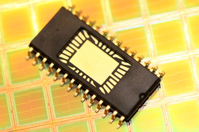
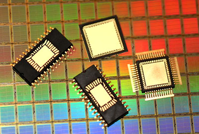
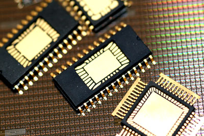
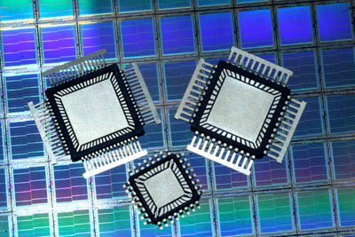
SEMPAC meets the latest JEDEC outline & footprint standards
Founded in 2000, SEMPAC provides innovative solutions in Semiconductor Packaging through the development and manufacturing of open cavity packages and B-Stage Lids. After working with customers in the integrated circuit assembly industry over the course of 25 years, the founders envisioned a market with a more reliable and less expensive alternative to the JEDEC compliant packages used for device prototyping and testing.
By leveraging our 50 years of combined experience in Semiconductor Assembly, we recognized the need for developing packaging solutions that did not require specialized equipment to assemble or require complicated storage requirements. By utilizing collaborative partnerships and working independently from the traditional contact manufacturing model, SEMPAC provides higher reliability solutions and is not in direct competition with our customers.
Through this ongoing partnership SEMPAC is continuing to develop innovative semiconductor packaging solutions for high frequency RF, optoelectronics, as well as power devices for both military and commercial applications. Our success is credited to our ongoing mission to provide high quality products and value while continuously working to improve our offerings so that they exceed our customer’s needs.
Available in QFN, QFP, and SOIC and SSOP architectures


